
SPI: What is the Serial Peripheral Interface Protocol?
关注、星标公众号,直达精彩内容
文章来源:https://www.engineersgarage.com/spi-what-is-serial-peripheral-interface-protocol/
整理:技术让梦想更伟大 | 李肖遥
SPI has earned a solid role in embedded systems whether it is system on chip processors, both with higher end 32-bit processors such as those using ARM, MIC or Power PC and with other microcontrollers such as the AVR, PIC etc. These chips usually include SPI controllers capable of running in either master or slave mode. In-system programmable AVR controllers can be programmed using an SPI interface. Chip or FPGA based designs sometimes use SPI to communicate. So, SPI is a common technology used nowadays for communication with peripheral devices where we want to transfer data speedily and with in real time constraints. There are many serial interfaces right from Morse code telegraphy, RS232, USB, Fire wire, Ethernet and many more. Each serial interface offers advantages or disadvantages for many designs, depending on criteria such as needed data rate, space availability, and noise considerations.
Serial to Peripheral Interface (SPI) was one such technology developed to replace parallel interfaces so we don’t have to route parallel bus around PCB. It provides high-speed data transfer between the devices. Motorola was the first company that named SPI to a circuit technique used in the late 1970s in its first 68000-based MCU to connect it to peripheral functions and later adopted by others in the industry. It’s the simplicity of interfacing and the speed that allows communication or transferring data easily and made it popular communication protocol.
The Serial Peripheral Interface is a simple 4-wire serial communications interface used by many microprocessor/microcontroller peripheral chips that enables the controllers and peripheral devices to communicate with each other. In Serial peripheral interface data is shifted in /out one at a time and transmit data from master device to/from one or more slave devices over short distances and high speed. It is simply based on an 8 bit shift register shifting data out on a single pin and shifting data in on another pin. Another feature of SPI is that there is no concept of transferring the ownership of the bus i.e. changing the master and also there are no slave addresses. SPI is a much simpler protocol and because of this we can operate it at speeds greater than 10MH as compared to TWI. Some of the features that allows SPI widely used are-
Full duplex communication.
Higher throughput than TWI.
Not limited to 8 bit words in the case of bit transferring.
Simple hardware interfacing
Arbitrary choice of message sizes, contents and purpose.
Typically low power requirements
Slave uses master’s clock and does not require precision oscillators.
Lower power requirements than TWI due to less circuitry.
However, it would be unfair to compare TWI serial interface to SPI. Each of them have their area of application depending on the need of the system like some of the features that makes TWI equally valuable as SPI.
Less number of pins on IC packages than SPI
Hardware flow control is present
It has a formal standard unlike SPI
It addresses slaves before communication.
Now, we have a brief idea on SPI let’s understand the answers to the questions about why SPI is most preferred in PCB? What are the basic connections and how do they communicate? And lastly what is the future scope of SPI?
Why is SPI more preferred more for PCB
Even though it is developed primarily for the communication between host processor and peripherals, a connection of two processors via SPI is just as well possible. The SPI Bus is usually used only on the PCB. There are many reasons which prevent us from using it outside the PCB area. Firstly SPI was designed to transfer data between various IC chips, at very high speeds. Due to this high-speed the length of the bus lines should not be too long, because it increases the reactance and the Bus becomes unusable. However, its possible to use the SPI Bus outside the PCB at low speeds, but this is not quite practical. The peripherals can be a Real Time Clocks, converters like ADC and DAC, memory modules like EEPROM and FLASH, sensors like temperature sensors and pressure sensors, or some other devices like signal-mixer, potentiometer, LCD controller, UART, CAN controller, USB controller and amplifier.
Data and control lines of the SPI and the basic connection:
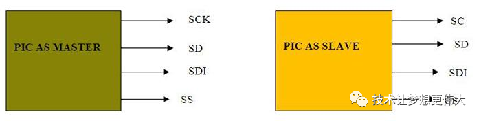
An SPI protocol specifies 4 signal wires.
Master Out Slave In (MOSI) – MOSI signal is generated by Master, recipient is the Slave.
Master In Slave Out (MISO) – Slaves generate MISO signals and recipient is the Master.
Serial Clock (SCLK or SCK) – SCLK signal is generated by the Master to synchronize data transfers between the master and the slave.
Slave Select (SS) from master to Chip Select (CS) of slave – SS signal is generated by Master to select individual slave/peripheral devices. The SS/CS is an active low signal.
Sometimes serial Data In [SDI] is used as another name in place of MOSI and Serial Data Out [SDO] for MISO.
Block Diagram Showing Single Master Single Master Application in SPI Protocol
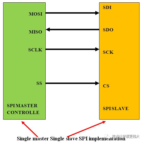
Among these four logic signals, two of them MOSI & MISO can be grouped as data lines and other two SS & SCLK as control lines.
A master-microcontroller can talk to multiple SPI Peripherals. There are 2 ways to set things up:
Cascaded slaves or daisy-chained slaves
Independent slaves or parallel configuration
Daisy-chained slave configuration
Daisy-chained slave configuration:In cascaded slave configuration, all the clock lines (SCLK) and chip select (CS) are connected together. The data flows out the microcontroller to each peripheral and back to the microcontroller. The data output of the preceding slave-device is tied to the data input of the next, thus forming a wider shift register. So the cascaded slave-devices are evidently looked at as one larger device and receive therefore the same chip select signal. This means, only a single SS line is required from the master, rather than a separate SS line for each slave.
Daisy-Chained Slave Configuration in SPI Protocol
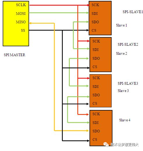
But we have to remember that the daisy-chain will not work with devices which support or require multiple bytes operation.
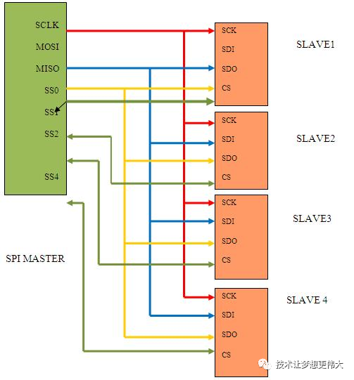
Independent slave configuration:
This is the typical SPI-bus configuration with one SPI-master and multiple slaves/peripherals. In this independent or parallel slave configuration,
All the clock lines (SCLK) are connected together.
2. All the MISO data lines are connected together.
3. All the MOSI data lines are connected together.
Block Diagram Displaying SPI Bus in Slave Configuration
Block Diagram showing various functional units in SPI system
Communication in SPI
How Does Communication in SPI Work?
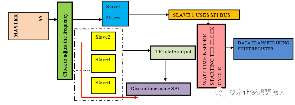
The communication is initiated by the master all the time. The master first arranges the clock by using a frequency, which is less than or equal to the maximum frequency that the slave device supports. Now, this SPI master controls the data transfer by generating the clock signal (SCLK).The master then select the desired slave for communication by pulling the chip select (SS) line of that particular slave-peripheral to “low” state and activates the particular slave it wants to communicate with by using slave-select signal (SS). Once slave is selected then receives or transmits data via the two data lines. A master, usually the host micro controller, always provides clock signal to all devices on a bus whether it is selected or not. The slaves on the bus that has not been activated by the master using its slave select signal will disregard the input clock and MOSI signals from the master, and must not drive MISO. That means the master selects only one slave at a time.
The usage of these each four pins may depend on the devices. For example, SDI pin may not be present if a device does not require an input (ADC for example), or SDO pin may not be present if a device does not require an output (LCD controllers for example). If a microcontroller only needs to talk to 1 SPI Peripheral or one slave, then the CS pin on that slave may be grounded. With multiple slave devices, an independent SS signal is needed from the master for each slave device.
What is the significance of Tri- state output in SPI?
In digital electronics three-state, tri-state, or 3-state logic allows an output port to assume a high impedance state in addition to the 0 and 1 logic levels, effectively removing the output from the circuit. This allows multiple circuits to share the same output line or lines (such as a bus which cannot listen to more than one device at a time. Most devices/peripherals have tri-state outputs, which goes to high impedance state (disconnected) when the device is not selected. Devices without these tri-state outputs cannot share SPI bus with other devices, because such slave’s chip-select may not get activated.
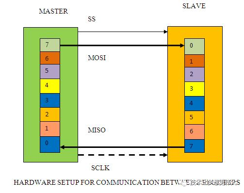
Now, if a waiting period is required (such as for analog-to-digital conversion) then the master must wait for at least that period of time before starting to issue clock cycles. In the master SPI, the bits are sent out of the MOSI pin and received in the MISO pin. The bits to be shifted out are stored in the SPI data register, SP0DR, and are sent out most significant bit (bit 7) first. When bit 7 of the master is shifted out through MOSI pin, a bit from bit 7 of the slave is being shifted into bit 0 of the master via the MISO pin. After 8 clock pulses or shifts, this bit will eventually end up in bit 7 of the master. The least significant bit can be sent out first by setting the LSBF bit to 1 in the SPI Control Register. The clock that controls how fast the bits are shifted out and into SP0DR is the signal SCLK. The frequency of this clock can be controlled by the SPI baud rate register, SP0BR. The SS pin must be low to select a slave. A complete SPI system is shown below.
Overview of communication in SPI System with master and slave
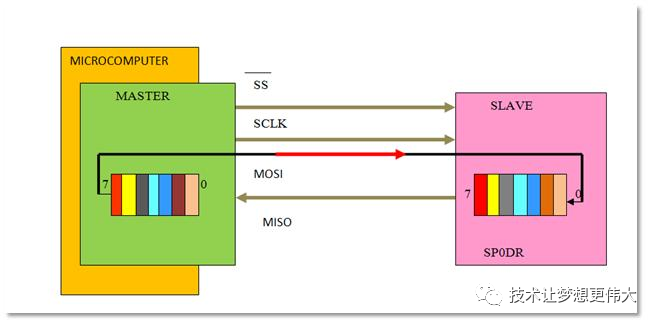
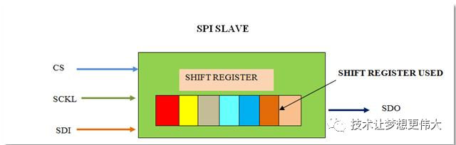
Diagram showing structure of SPI Slave
A full duplex means data transmission can occur in both directions during each clock cycle. So, when the master sends a bit on the MOSI line; the slave reads it from that same line and the slave sends a bit on the MISO line; the master reads it from that same line. Now, to make data transfer organized shift registers are used with some given word size such as 8 bit (can be more) in both master and slave. They are connected in a ring. While master shifts register value out through MOSI line, the slave shifts data in to its shift register.
Data are usually shifted out with the MSB-most significant bit first, while shifting a new LSB- least significant bit into the same register. After that register has been shifted out, the master and slave have exchanged their register values. Then each device takes that value and does the necessary operation with it (for example, writing it to memory). If there are more data to be exchanged, the shift registers are loaded with new data and the process is repeated. When there are no more data to be transmitted, the master stops its clock. Normally, it then rejects the slave.
Block Diagram Showing Hardware Setup For Communication Between 2 Registers
There is a “multiple byte stream mode” available with SPI bus interface. In this mode the master can shift bytes continuously. In this case, the slave select (SS) is kept low until all stream process gets finished.
SPI devices sometimes use another signal line to send an interrupt signal to a host CPU. Some of the examples for these type of signals are pen-down interrupts from touch-screen sensors, thermal limit alerts from temperature sensors, alarms issued by real time clock chips, and headset jack insertions from the sound codec in a cell phone.
Clock polarity and phase in SPI
Significance of the clock polarity and phase:
Another pair of parameters called clock polarity (CPOL) and clock phase (CPHA) determines the edges of the clock signal on which the data are driven and sampled. In addition to setting the clock frequency, the master must also configure means adjusts or sets the clock polarity (CPOL) and phase (CPHA) with respect to the data. Since the clock serves as synchronization of the data communication, there are four possible modes that can be used in an SPI protocol, based on this CPOL and CPHA.
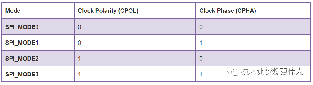
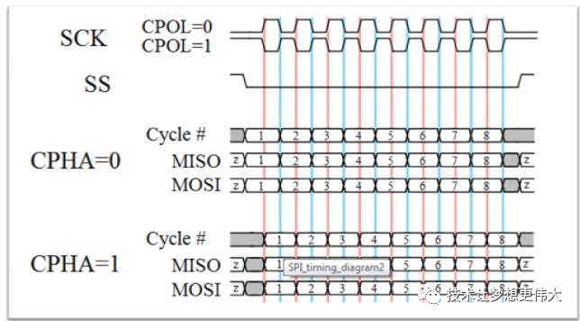
If the phase of the clock is zero (i.e. CPHA = 0) data is latched at the rising edge of the clock with CPOL = 0, and at the falling edge of the clock with CPOL = 1.
If CPHA = 1, the polarities are reversed. Data is latched at the falling edge of the clock with CPOL = 0, and at the rising edge with CPOL = 1.
The micro-controllers allow the polarity and the phase of the clock to be adjusted. A positive polarity results in latching data at the rising edge of the clock. However data is put on the data line already at the falling edge in order to stabilize. Most peripherals, which can only be slaves, work with this configuration. If it should become necessary to use the other polarity, transitions are reversed.
APPLICATIONS OF SPI
The full duplex capability makes SPI very efficient for master/slave applications. Some devices use the full-duplex mode to implement an efficient, swift data stream for applications such as digital audio, digital signal processing, or telecommunications channels. SPI is used to talk to variety of peripherals, such as
Sensors: Temperature, pressure, ADC, touch-screens, video game controllers
Control devices: Audio coding and decoding, digital potentiometers, DAC.
Camera lenses: Canon EF lens mount
Communications: Ethernet, USB, USART, CAN handheld video games
Memory: Flash and EEPROM
Real-time clocks
LCD, sometimes even for managing image data
Any MMC or SD card (including SDIO variant)
For high performance systems, FPGAs sometimes use SPI to interface as a slave to a host, as a master to sensors, or for flash memory used to bootstrap if they are SRAM-based.
JTAG is essentially an application stack for a three-wire SPI flavor, using different signal names. SGPIO is essentially another (incompatible) application stack for SPI designed for particular backplane management activities SGPIO uses 3-bit messages.
‧‧‧‧‧‧‧‧‧‧‧‧‧‧‧‧ END ‧‧‧‧‧‧‧‧‧‧‧‧‧‧‧‧
关注我的微信公众号,回复“加群”按规则加入技术交流群。
点击“阅读原文”查看更多分享,欢迎点分享、收藏、点赞、在看。